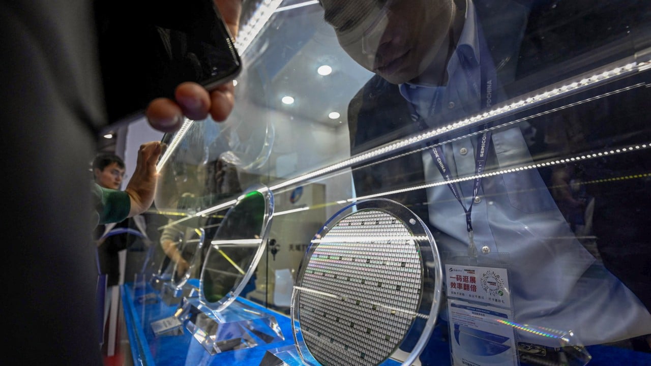
Capital expenditure in the semiconductor sector operates on a temporal asymmetry. Facilities financed today do not yield functional silicon until years later, requiring firms to commit tens of billions of dollars against forecasted multi-year compute requirements. SK Hynix board approval of a 54 trillion won, or roughly 38 billion dollar, outlay for two domestic fabrication plants in Yongin and Cheongju illustrates this capital deployment strategy. This financial commitment targets structural bottlenecks in artificial intelligence hardware supply chains rather than cyclical consumer electronics demand. Deconstructing this allocation requires examining the underlying cost functions of high-bandwidth memory production, the physical constraints of fab construction, and the economic shifts governing modern data center architectures.
The Cost Structure of Advanced Semiconductor Fabrication
Building modern semiconductor manufacturing cleanrooms involves capital distribution across distinct operational vectors: civil engineering, lithography tool procurement, cleanroom infrastructure, and yield stabilization. The 38 billion dollar investment is split unevenly across two distinct assets, reflecting the differing unit economics of dynamic random-access memory and NAND flash production.
The Yongin Y2 facility commands 35.2 trillion won, representing roughly two-thirds of the total capital expenditure. This facility is engineered for advanced dynamic random-access memory and high-bandwidth memory production. High-bandwidth memory assembly departs from traditional memory manufacturing through advanced packaging techniques, specifically silicon via technology and thermal compression bonding. These steps require specialized cleanroom environments and precision bonding equipment that increase capital intensity per square meter.
The Cheongju M17 facility absorbs the remaining 19.1 trillion won, dedicated to NAND flash manufacturing. While enterprise solid-state drive demand scales alongside artificial intelligence processing nodes to handle large training datasets, NAND capital expenditure efficiency differs from logic or high-bandwidth memory. The vertical scaling of flash memory relies on stacking increasing numbers of cell layers, shifting the cost bottleneck from lithography exposure tools to etch and deposition precision.
The Temporal Lag and Supply Chain Bottlenecks
The structural timeline of semiconductor expansion introduces a severe lag between financial authorization and operational output. Groundbreaking for the Cheongju M17 plant is scheduled for February 2027, with cleanroom activation targeted for December 2028. The larger Yongin Y2 plant breaks ground in July 2027, projecting cleanroom availability by June 2029.
This multi-year timeline creates an interval of supply vulnerability. High-bandwidth memory supply chains are currently constrained, with capacity committed well in advance across the industry. When demand for artificial intelligence accelerators accelerates faster than fab buildout timelines, buyers face allocation limits.
The physical constraints governing this timeline include:
- Cleanroom particulate certification schedules
- Lead times for extreme ultraviolet and deep ultraviolet lithography systems
- Utility hookups requiring dedicated regional power and water purification infrastructure
- Yield ramp duration required to achieve economically viable defect densities
Firms cannot accelerate this timeline by simply increasing capital injection. The constraint shifts from financial liquidity to equipment manufacturer throughput and specialized engineering labor availability.
Structural Demand Versus Cyclical Volatility
Historically, memory manufacturers experienced severe boom-and-bust cycles tied to personal computer and smartphone replacement rates. Excess supply caused pricing collapses, forcing prolonged capital expenditure freezes. The current capital allocation cycle represents a structural divergence from this historical pattern.
Artificial intelligence data centers treat memory not as a commoditized storage medium, but as a core determinant of accelerator performance. Processor utilization rates depend on memory bandwidth. If an accelerator starves for data, expensive compute logic sits idle. This operational dependency shifts the economic value proposition. End-users prioritize guaranteed volume and thermal-electrical stability over marginal unit cost reductions.
Market forecasters project compound annual growth rates for memory demand through 2030, driven by larger parameter models and agentic workflow execution. This institutional shift underpins the rationale for a 38 billion dollar capital commitment. The risk is not a temporary dip in consumer device sales, but the potential miscalculation of hyperscale infrastructure spending trajectories over a three-to-five-year horizon.
Balance Sheet Mechanics and Risk Mitigation
Funding a multi-year, multi-billion-dollar infrastructure project requires rigorous cash flow management to avoid over-leveraging during economic contractions. Operating margins reaching historical highs provide the internal liquidity required to fund these capital projects without excessive debt accumulation.
When cash generation matches capital expenditure velocity, firms retain strategic autonomy. Competitors constrained by debt servicing costs must rely on credit markets, exposing them to interest rate fluctuations and capital market tightening. Maintaining a robust balance sheet allows manufacturers to sustain fab construction schedules even if macroeconomic indicators soften mid-cycle.
Strategic execution requires continuous monitoring of yield curves, advanced packaging yield rates, and shifts in accelerator architectures. As next-generation packaging standards transition toward hybrid bonding, capital allocation must remain flexible enough to retool cleanroom interiors without stranding initial civil engineering investments.
Prioritize procurement synchronization with primary processor designers to align cleanroom readiness dates with commercial silicon tape-outs, ensuring that newly activated square footage immediately transitions to volume manufacturing.